Product number:2501798
Date:2024-09-24
Views:1,068
Product Introduction: for you to see more, deeper, more accurate! High-precision laser confocal measurement of three-dimensional surface topography Large Depth Subsurface Defects Sub-surface detection
for you to see more, deeper, more accurate!
High-precision laser confocal measurement of three-dimensional surface topography
Large Depth Subsurface Defects
Sub-surface detection depth up to 100 μm!
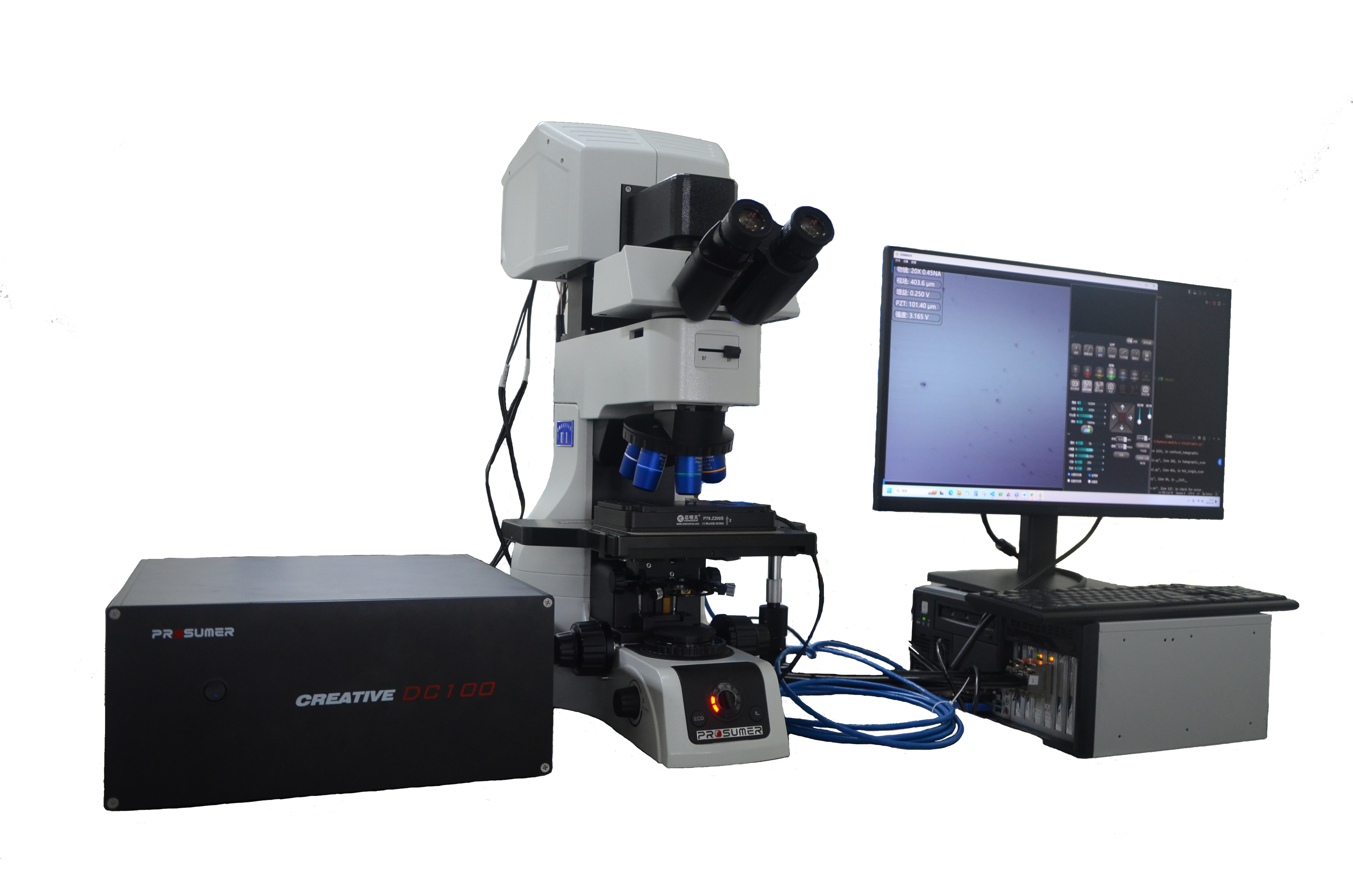
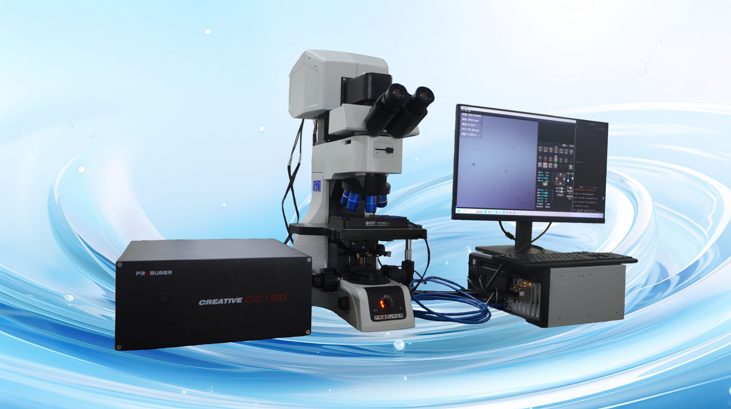
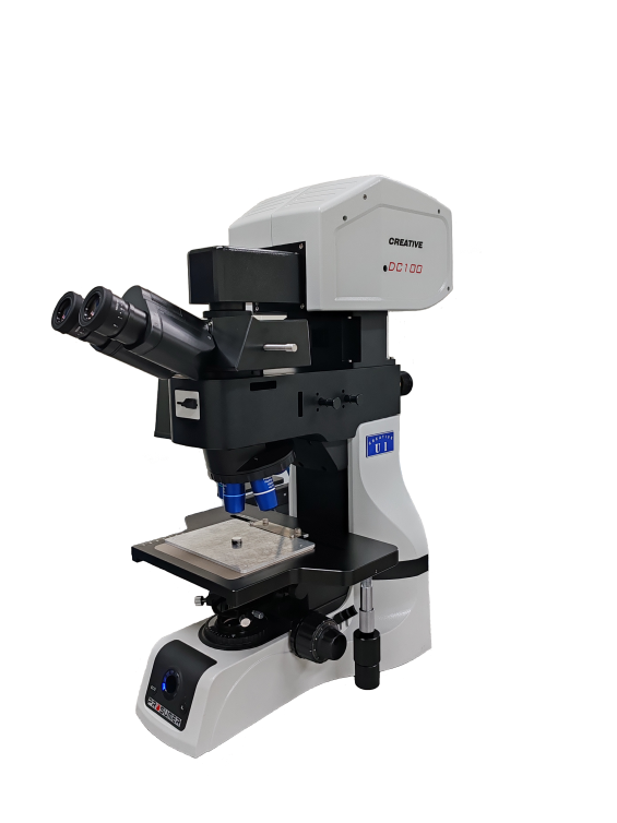
DC100 confocal microscope is a new generation of high-end stereo microscopic measuring instrument developed by Spectra Sima Instruments. It is a high-end three-dimensional microscopic instrument with both surface topography measurement and sub-surface defect detection capabilities. It can be widely used for surface quality detection such as roughness and cracks in the field of metal processing, and for microstructure three-dimensional size and sub-surface defect detection in the field of semiconductor devices, MEMS components, photovoltaic panels, ultra-precision parts and LED, optical surface profile measurement and sub-surface defect detection in the field of advanced optical processing, material surface structure characterization in the field of material manufacturing and research and development, etc.
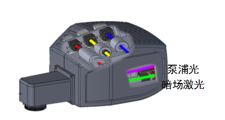
fusion of three measurement methods in one
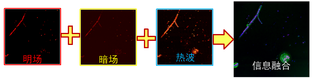
multi-modal measurement (optional)
Fusion of confocal bright field, confocal dark field, three-dimensional true color and thermal wave imaging methods to obtain more abundant information on the sample surface and subsurface
brightfield confocal imaging
Point illumination and point detection realize the separation of quasi-focus and out-of-focus signals, and realize three-dimensional imaging.
High-sensitivity confocal peak positioning algorithm to achieve nanoscale axial resolution

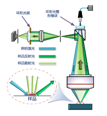
dark-field confocal imaging
Through the ring light shaping module and complementary aperture, the surface reflected light and sub-surface scattered light are separated, and the three-dimensional distribution information of sub-surface defects is obtained.
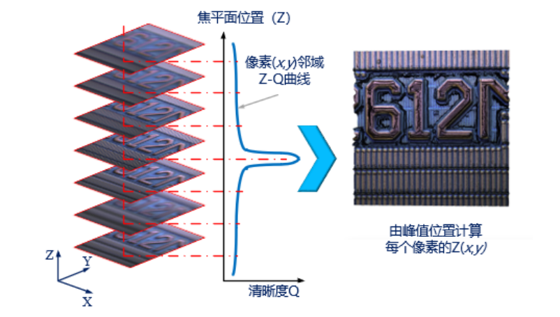
three-dimensional true color imaging
Take sample photos along the Z direction, judge the Z position of each pixel according to the clarity, and obtain the sample shape data containing real colors.
Simplifies the measurement process
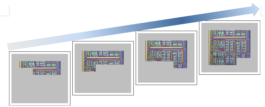
Full Range Map Navigation
The area captured by a single shot can be displayed and recorded on the map, which is convenient for users to find out the whole picture of the sample. Click the mouse in the map to make the displacement stage move the area corresponding to the sample to the center of the picture.
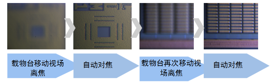
autofocus
The automatic focusing function of the microscope makes it possible to reduce the manual adjustment operation as much as possible during the measurement process, and can quickly and easily obtain a clear in-focus image
simple image processing
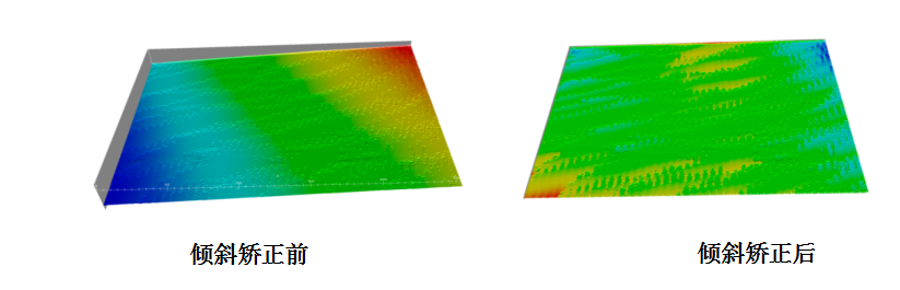
Tilt correction: solve the problem of tilting the measured area and make the height information more accurate and clear
morphology filtering: Filter out abnormal measurement points and reduce noise interference on data
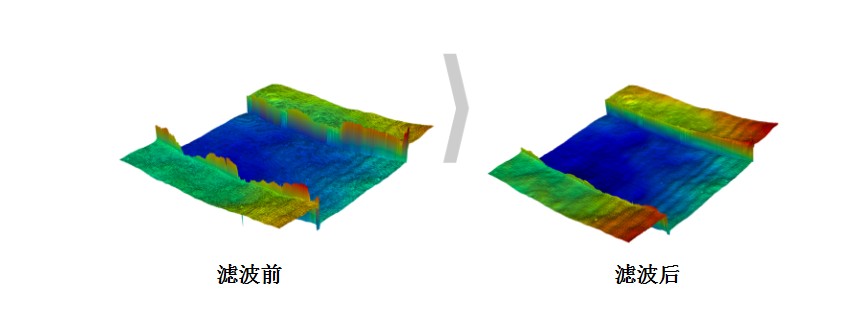
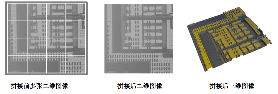
image mosaic: Combined with the position data of the displacement stage, large sample measurement is realized by image stitching
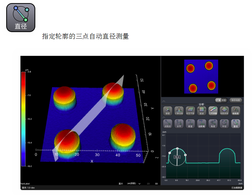
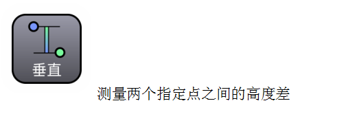
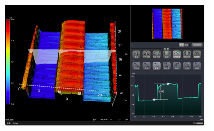
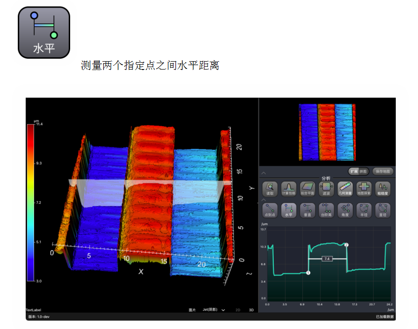
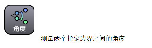
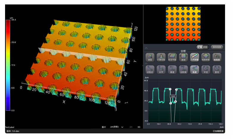
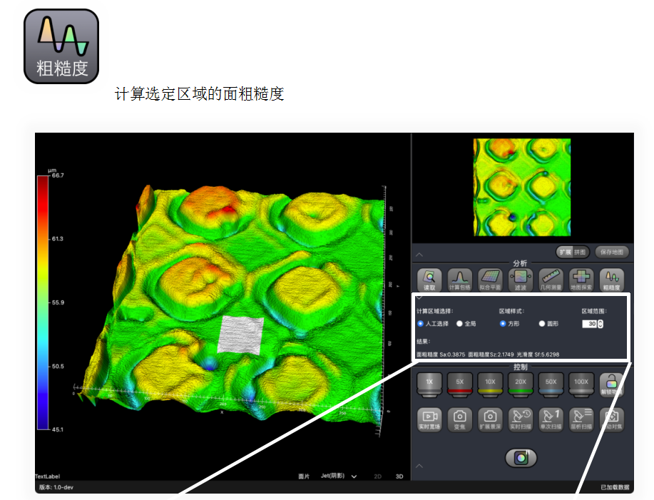
Intuitive Image Analysis
Typical application scenarios
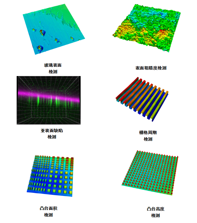
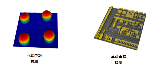
This microscope can be used as an observation and analysis instrument for scientific research departments and production units, and is also an ideal instrument for assisting precision micro-nano processing and semiconductor production research and development. It can be widely used in metal materials, integrated circuits, electronic chips, optical glass and other shape measurement and defect detection.
contacts: Mr Luo.
mobile phone: +7(925)539-89-20
telephone: +7(925)539-89-20
address: